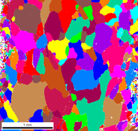
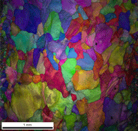
Grain size measurement by electron backscattered diffraction (EBSD) has several unique advantages over the traditional measurement of etched specimens by the light optical microscopy (LOM) approach as defined in ASTM E 112. This is most evident when trying to measure the grain size of twinned face-centered cubic (FCC) metals where two major problems are encountered. First, in many cases, it is difficult to reveal a very high percentage of the grain boundaries by etching. Secondly, nearly all etchants for twinned FCC metals do reveal the twin boundaries and one must ignore the twin boundaries when measuring the grain size by LOM. The notable exception to this experience is electrolytic etching of the 300 series of austenitic stainless steels where Bell and Sonon’s aqueous 60% nitric acid [1], using a platinum cathode and a voltage no greater than 1.5 V DC will reveal nearly 100% of the grain boundaries and virtually none of the twin boundaries. Another significant problem that affects EBSD results somewhat more than LOM etching results is the greater difficulty in preparing the highly ductile FCC metals to the perfection needed to get a very high percentage of the pixels to be indexable. Specimen preparation [2-4] is a very critical step in getting a very high percentage of indexable pixels in the field of view. This is not a trivial matter.
To do grain size measurements by EBSD, a properly polished, non-etched, damage-free, representative field is scanned, pixel by pixel, developing a diffraction pattern at each pixel position. A typical scan can run 10 to 20 minutes, although longer times may be required for some microstructures. The system then looks for variations in the diffraction patterns over the scanned region. A grain is defined by all the adjacent pixels with the same diffraction pattern within a certain degree of mis-orientation. A grain boundary is defined by the boundary angle between two adjacent regions with the same orientation within each region, but a different orientation across a shared boundary. In this way the system creates a grain structure map. Twin boundaries can also be identified as the orientation across a twin boundary is unique and the angle across a twin boundary is much smaller than across a grain boundary. All metallographers working with FCC metals and alloys will instantly recognize the value of this technique as delineation of all of the grain boundaries in FCC metals and alloys is very difficult and twin boundaries can be difficult to discriminate from grain boundaries when trying to measure their grain size.
Metals and alloys are generally of three crystal structures: body-centered cubic (BCC), face-centered cubic, or hexagonal-close packed (HCP). Annealing twins are observed in most FCC metals and alloys (except for Al) after deformation and annealing. An occasional twin boundary may be seen in an as-cast FCC metal, but these are due to growth accidents. HCP metals and alloys deform by mechanical twinning (rather than by slip, as FCC and BCC metals). BCC metals do not form annealing twins, but under extreme conditions of low temperature and high strain rate can form mechanical twins. In general, it is easier to etch a BCC metal to reveal the grain structure by LOM to a level that permits a precise measurement.
 |
 |
 |
| a) | b) | c) |
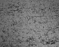
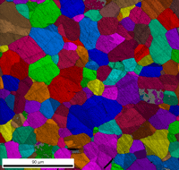
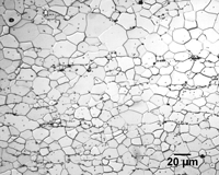
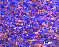
| Figure 1. Motor lamination steel before decarburization etched with (a) Marshall’s reagent and then 2% nital; (b) Klemm’s I; and (c) the combined index of quality and grain orientation map. | ||
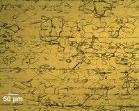
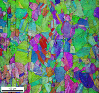
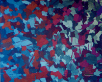
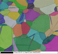
Figure 1 shows the microstructure of a BCC motor lamination sheet steel where the grain structure is well developed using Marshall’s reagent [5] and enhancing the attack with nital. Color etching with Klemm’s I reagent [6, 7] fully revealed the grain structure, but image analysis systems cannot easily handle color, so manual measurements are required. The combination of a grain orientation map, which colors the grains according to their crystal orientation, and an index of quality (IQ) map, which reveals the grain boundaries, is used to define the grains, followed by determining the area of each grain, calculation of an average grain size and the ASTM grain size number per E 112. The chief disadvantage of this technique is the scanning time needed to obtain data for 500 or more grains. The speed to perform the detection has improved over the past ten years. Currently, because BCC metals usually can be etched easily obtaining a high percentage of the grain boundaries, there is less need to use EBSD for such specimens, unless etching is a problem.
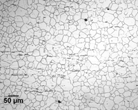
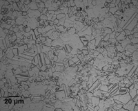
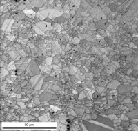
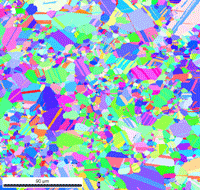
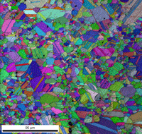
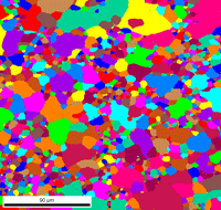
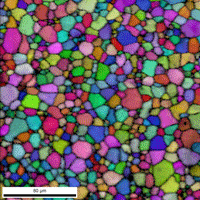
Figures 2 and 3 show much more difficult subjects, the grain structure of FCC tough-pitch copper and FCC 316 stainless steel. The standard etchants are completely inadequate while the color etch can only be measured manually, and with difficulty. The special electrolytic etch for stainless steel works very well, but there are similar etchants for only a few Ni-based twinned FCC metals. Except perhaps for the austenitic stainless steels and a few Ni-base superalloys, the EBSD grain size technique offers great value in that precise measurements of grain size can be obtained in FCC (and also in HCP metals with mechanical twins).
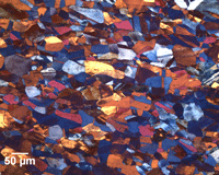
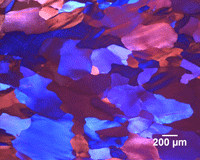
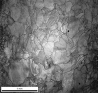
Figure 4 shows cold worked and solution annealed (1000°C) nickel-based Alloy 625 which contains annealing twins. The LOM image in Fig. 4a exhibits only partial delineation of the grain structure. In Figure 4 b, EBSD has been used to detect the grain and twin boundaries in black and white with an index of quality map. In Fig. 4c a grain orientation map is shown where the colors relate to the crystal orientation within the grains and twins. In Fig. 4d, the index of quality and grain orientation maps have been combined, while in Fig. 4e, the twin boundaries have been removed permitting grain area measurements. Figure 5 shows mechanical twinning in HCP commercial purity titanium, ASTM F67, Grade 2. When properly polished, CP Ti responds very well to polarized light, Fig. 5a, and the grain structure and mechanical twins can be seen without etching.
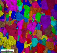
Fig. 5b shows the use of the Euler orientations to color the grains and the mechanical twins. Figure 6a shows deformed high-purity iron (99.98% Fe) after etching with Klemm’s I color tint etch. The distorted grain shapes are due to the prior deformation. Figure 6b shows an index of quality map revealing the grain structure of the as-polished specimen. Figure 6c shows the colored grain orientation map and Figure 6d shows the combined index of quality and grain orientation map permitting measurement of the area of each grain. Note that the outer edges of the image, which were more highly deformed, had pixels that would not yield acceptable quality diffraction patterns.
Conclusions
Electron backscatter diffraction analysis is an exceptionally powerful tool. In this article, the detection of grain structure was illustrated for FCC metals containing annealing twins, for non-twinned BCC metals and for an HCP metal with mechanical twins. Specimen preparation is critical to obtaining excellent results. All damage introduced during specimen preparation must be removed and the surface flatness must be excellent. Only as-polished specimens are used for EBSD. The procedure can also be used to identify phases and to study crystal orientation.
References
1. F. C. Bell and D. E. Sonon, “Improved Metallographic Etching Technique for Stainless Steel and for Stainless Steel to Carbon Steel Weldments,” Metallography, Vol. 9, 1976, pp. 91-107.
2. G. F. Vander Voort, “Metallographic Specimen Preparation for Electron Backscatter Diffraction, La Metallurgia Italiano, Vol. 101, November – December 2009, pp 71-79.
3. G. F. Vander Voort, “Metallographic Specimen Preparation for Electron Backscattered Diffraction – Part 1,” Practical Metallography, Vol. 48, No. 9, September 2011, pp. 454-473.
4. G. F. Vander Voort, “Metallographic Specimen Preparation for Electron Backscattered Diffraction – Part 2,” Practical Metallography, Vol. 48, No.10, October 2011, pp. 527-543.
5. D. N. Hawkins, “An Etchant for Revealing the Substructure in Low-Carbon Steels,” Metallography, Vol. 14, 1981, pp. 61-68.
6. M. Beckert and H. Klemm, Handbook of Metallographic Etching Methods, Veb Deutscher Verlag für Grundstoff, Leipzig, 1962.
7. H. Klemm, “Uses of Sodium Thiosulfate (Klemm’s Reagent) as an Etchant,” Praktische Metallographie (Practical Metallography), Vol. 5, April 1968, pp. 163-177..
George Vander Voort has a background in physical, process and mechanical metallurgy and has been performing metallographic studies for 47 years. He is a long-time member of ASTM Committee E-4 on metallography and has published extensively in metallography and failure analysis. He regularly teaches MEI courses for ASM International and is now doing webinars. He is a consultant for Struers Inc. and will be teaching courses soon for them. He can be reached at 1-847-623-7648, EMAIL: georgevandervoort@yahoo.com and through his web site: www.georgevandervoort.com
To View a listing of all George’s articles please click here
Read George Vander Voort’s Biography

